Inside the ESP32: From Xtensa Cores to Dumping the Flash
A practical walkthrough of what is actually inside the ESP32: its Xtensa cores, memory map, boot flow, and what you can recover by dumping the flash.
- Published
- Nov 11, 2025
- Read Time
- 17 min read
- Words
- 3,681
- views
- —
- Author
- @zuanki
Activity
views/week
last 24 weeks
Activity
views/week
last 24 weeks
TL;DR
- The ESP32 is much more than a “simple microcontroller” — it is a small SoC with dual Xtensa cores, a ULP coprocessor, flash mapping, and a fairly interesting boot flow.
- Its limited SRAM is not the full story: a lot of the magic comes from memory mapping and cache.
- If flash encryption is not enabled, dumping the flash can reveal a lot more than you might expect, including Wi-Fi credentials.
The ESP32 Is Not “Just” a Microcontroller
I recently got my hands on an ESP-WROOM-32, and one question immediately came to mind: what is actually inside this thing?
Most people first meet the ESP32 through a tiny demo — blink an LED, connect to Wi-Fi, maybe read a sensor, and move on. That makes it feel like a small and fairly ordinary microcontroller. That description is technically fine, but it hides a lot. The ESP32 is not just a chip that toggles GPIO pins and talks to a UART. It is a complete SoC (System-on-a-Chip) manufactured on a 40nm process, with enough moving parts to make it much more interesting than it first looks.
On one small chip, you get:
- Wi-Fi (2.4 GHz band)
- Bluetooth (Classic and BLE)
- Dual high-performance CPU cores
- An Ultra-Low-Power coprocessor
- A fairly involved memory system
- A lot of peripherals
That is quite a lot of machinery for a chip many people first encounter through an Arduino sketch.
In this article, I want to peel that machinery apart a bit. We will start with the CPU architecture, then look at memory and boot flow, and finally get to the part I cared about most: dumping the firmware and checking what is actually stored in flash.
Why Xtensa, and Not ARM?
The first weird thing about the ESP32 is that it does not use ARM.
If you come from the world of STM32, RP2040, or many other embedded platforms, ARM feels like the obvious default. But the ESP32 instead uses the Tensilica Xtensa LX6 CPU.
This is interesting because Xtensa is not just “another CPU core”. Unlike fixed ISAs such as ARM or x86, Xtensa is a configurable architecture. That means chip vendors can license the architecture and tailor parts of it to fit the kind of workloads they care about. They can add instructions, tune features, and optimize the core for specific use cases such as DSP-heavy work, control logic, or cryptographic operations.
In other words, Espressif did not just pick a CPU. They picked a CPU family that is designed to be shaped.
That flexibility is a big deal in embedded systems. It lets vendors avoid building a separate accelerator for every little thing while still getting some of the benefits of hardware-level optimization. Of course, the trade-off is that Xtensa is less familiar to many developers than ARM, and the ecosystem around it feels more vendor-specific. Still, for a chip like the ESP32, the choice makes sense.
Two Cores, but Not Quite as Symmetric as It Sounds
The ESP32 contains two identical Xtensa LX6 CPUs. On paper, this is a Symmetric Multiprocessing (SMP) system: both cores share most of the memory and peripherals, and both are coordinated by FreeRTOS, a real-time operating system.
That is the official description, and it is correct. In practice, though, the split is often much less “symmetric” than that wording suggests.
The two cores are usually referred to as:
- CORE 0 (PRO_CPU): Short for “Protocol CPU”. This core typically handles protocol-heavy work such as the Wi-Fi stack and Bluetooth stack.
- CORE 1 (APP_CPU): Short for “Application CPU”. This is where user application code usually runs.
This division is practical, not magical. The Wi-Fi and Bluetooth stacks are timing-sensitive systems. They are expected to react quickly, and they do not like being blocked for too long. So even though the hardware is symmetric, software convention gives the cores different personalities.
That difference matters.
You can run your own code on PRO_CPU, but you should be careful. If you put a badly behaved task there — for example, something that blocks for too long, spins unnecessarily, or does a delay(1000) in the wrong place — you are not “just making one core busy”. You are interfering with work that is often responsible for keeping the radio side alive. That can mean dropped packets, unstable connectivity, or timing problems that are annoying to debug.
This is where FreeRTOS comes in. FreeRTOS is the layer that schedules tasks across the cores, lets them communicate safely, and provides synchronization mechanisms like Queues, Semaphores, and related primitives. It is the traffic controller that stops your dual-core system from becoming a race-condition machine.
The Tiny Third Brain: ULP
The ESP32 also has a third, much smaller “brain”: the ULP (Ultra-Low-Power) Coprocessor.
This part is cool because it keeps working when the main CPUs are asleep.
The ULP is essentially a programmable FSM (Finite State Machine) operating in the RTC (Real-Time Clock) domain. It can be programmed in assembly using tools such as esp32ulp-assembler, and its whole purpose is to do tiny, low-power tasks while the big cores stay off.
That is the important part. While the two main Xtensa cores are in deep sleep, the ULP can still:
- Read sensors
- Check thresholds or simple logic conditions
- Keep a tiny bit of state
- Wake the main CPUs only when necessary
This is one of the reasons the ESP32 works so well in battery-powered IoT devices. You do not have to wake the full system just to ask, every few seconds, “has this sensor value crossed a threshold yet?”
The ULP uses two RTC-related memory regions:
- RTC_FAST_MEM (8 KB): stores the ULP’s instructions
- RTC_SLOW_MEM (8 KB): stores retained data and state during deep sleep
So yes, the ESP32 has two main application cores. But it also has this much smaller helper that quietly keeps watch when the rest of the chip is mostly asleep. That is not something you expect if you only know the chip from beginner Wi-Fi examples.
Memory: Where Code Actually Runs
This is one of the easiest parts to misunderstand, so it is worth slowing down here.
The ESP32 is a dual-core system with two Xtensa LX6 CPUs following a Harvard Architecture. That means instructions and data travel on separate buses. The chip has an instruction bus and a data bus, and memory or peripherals can be mapped onto one or both depending on what kind of access is needed.
That sounds abstract, but it matters because it shapes how the ESP32 sees the world. The CPUs do not deal with “RAM here, flash there, peripherals somewhere else” in the same human-friendly way we describe them. Instead, they see address spaces, and the chip designer decides what lives behind each region.
Address Space: 4 GB Does Not Mean 4 GB of RAM
The ESP32 exposes a 32-bit address space for both the instruction bus and the data bus. That gives each bus a theoretical address range of 4 GB.
This does not mean the ESP32 has 4 GB of RAM. Not even close.
It only means the CPU can generate addresses across a 4 GB range. What actually exists behind those addresses is a separate question. Some addresses map to ROM, some to SRAM, some to external memory, some to peripherals, and some to special hardware regions.
That distinction is extremely important:
- Addressable space is what the CPU can point at.
- Physical memory is what actually exists on the chip or outside it.
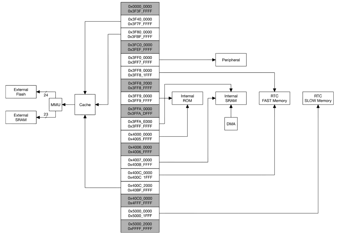
On the ESP32, this address space is divided into regions such as:
- 1296 KB for Embedded Memory
- 19704 KB for External Memory
- 512 KB for Peripherals
- 328 KB for DMA (Direct Memory Access)
The exact map is not the main thing to memorize here. The important idea is that the CPU sees one large addressable universe, and Espressif decides which parts of that universe correspond to ROM, SRAM, flash, peripherals, and DMA-related windows.
Embedded Memory (On-Chip)
This is the memory physically inside the ESP32 chip itself. It is the fastest memory the CPU can access directly, and it is where the most performance-sensitive work lives.
The ESP32 includes:
- 448 KB Internal ROM: very fast, but read-only. This contains the First-Stage Bootloader and various low-level support routines.
- 520 KB Internal SRAM: this is where important code and data live at runtime. It is divided into IRAM (Instruction RAM) and DRAM (Data RAM).
- 8 KB RTC FAST Memory: used in the RTC domain, including by the ULP.
- 8 KB RTC SLOW Memory: retains state during
deep sleep.
This is the memory that makes the chip feel “alive” at runtime. ROM gets the machine started, SRAM holds hot code and data, and the RTC memories keep a tiny corner of the system awake when the rest is sleeping.
External Memory (Off-Chip)
Now we get to the part that looks impossible at first sight.
The ESP32 only has about 520 KB of internal SRAM, yet real applications can easily be multiple megabytes in size. My ESP-WROOM-32 module, for example, has 4 MB of external SPI flash. So where does that code actually “run”?
Not by loading the whole thing into SRAM. That would obviously not fit.
Instead, the ESP32 maps external memory into its address space and uses part of internal memory as a transparent cache.
The external memory support includes:
- Up to 16 MB of off-chip SPI Flash
- Up to 8 MB of off-chip SPI SRAM (less common, but supported for RAM expansion)
This is where the chip starts to feel clever. The application binary sits in flash, but the CPU can still execute it thanks to a combination of address mapping, MMU behavior, and cache. The chip makes external flash feel usable for code execution without pretending it is as fast as internal SRAM.
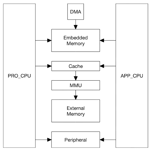
The block diagram in Figure 1 shows the system structure, and Figure 2 shows the address map structure.
At first sight, this sounds impossible: how does a chip with roughly 520 KB of SRAM execute an application that lives in several megabytes of flash?
The answer is that it does not load the entire application into SRAM. It maps flash into the address space and uses SRAM as instruction/data cache.
That is the trick.
The ESP32 uses part of its Embedded Memory as a transparent cache for external SPI flash. Roughly speaking, the flow looks like this:
- A CPU tries to fetch an instruction from an address that maps to external flash.
- The memory system checks whether the needed block is already in cache.
- If it is, execution continues quickly.
- If it is not, a cache miss occurs.
- The CPU stalls briefly while the memory controller reads a block from SPI flash and fills the cache.
- Execution resumes from the cached block.
This mechanism is what makes it possible to run software that is much larger than the internal SRAM alone would allow.
So when people say “the ESP32 has 520 KB of SRAM”, that is true, but it is not the whole story. The chip gets away with much more than that number suggests because it leans heavily on flash mapping and cache.
For exact address regions and register definitions, the ESP32 Technical Reference Manual is the authoritative source. The important thing for a mental model, though, is simpler: internal memory is precious and fast, external flash is larger and slower, and the cache system is what bridges the two.
How the ESP32 Boots
So how do ROM, flash, SRAM, and the cache machinery actually come together when the chip starts?
The boot process is where the pieces finally click.
On power-up, the CPU does not magically know where your application is. It begins from a fixed location and follows a staged handoff process:
- Stage 1 (ROM): The Xtensa CPU wakes up and starts executing from a fixed address in Internal ROM. This code is the First-Stage Bootloader, and you do not get to change it.
- Check Boot Mode: The ROM bootloader reads the strapping pins to decide how to continue — for example, boot normally from flash or enter a download/programming mode over UART.
- Stage 2 (Flash → IRAM): In a normal boot, the ROM code loads the Second-Stage Bootloader from flash, usually from address
0x1000, into executable memory and starts running it. - Read Partition Table: The second-stage bootloader then reads the Partition Table, usually located at
0x8000, to understand how the flash is laid out. - Load Application: Finally, it locates the application partition, sets up the memory mapping/MMU behavior and cache as needed, and transfers control to the application.
This staged flow is a very clean example of how the ESP32’s memory hierarchy is actually used:
- ROM gets the system off the ground.
- Flash stores the bootloader and application image.
- SRAM / IRAM / DRAM provide fast working memory.
- MMU and cache make larger flash-resident applications practical.
This is the mental model to keep: ROM starts the machine, flash stores the software, SRAM is where hot code and data live, and the mapping/cache layer makes the whole system feel larger than it physically is.
MMIO: How the CPU “Talks” to Hardware
Here is one of my favourite ideas in embedded systems: the CPU does not know what a GPIO pin is.
It does not know what UART is either. Or SPI. Or I2C.
All the CPU really knows how to do is:
- Execute instructions
- Read from memory
- Write to memory
So how does it control a pin, talk to a serial port, or configure a peripheral?
The answer is Memory-Mapped I/O (MMIO).
A portion of the ESP32’s address space is not connected to ordinary RAM at all. Instead, it is connected directly to hardware registers inside peripherals.
For example:
- An address range around
0x3FF44000maps to the GPIO hardware. - An address range around
0x3FF40000maps to UART0 hardware.
When software writes to one of these addresses, the CPU thinks it is just performing a memory write. But the hardware interprets that write as “set this bit”, “enable this peripheral”, “clear this interrupt”, or “toggle this output”.
So a high-level call like:
digitalWrite(LED_PIN, HIGH);eventually turns into something much closer to:
WRITE(SOME_GPIO_REGISTER, SOME_BITMASK);The CPU does not see that as “turn LED on”. It just sees “write value X to address Y”.
That is the trick. Talking to a peripheral does not look special to the CPU. It looks like another memory access. The hardware is what makes that memory access mean something.
This is why low-level embedded programming often feels like “just reading and writing registers”. Because in the end, that is exactly what it is.
"Hello, Wi-Fi!"
That is enough architecture for now. I wanted to see something concrete, so I flashed the simplest useful program I could think of: connect to Wi-Fi and print the result.
I used PlatformIO to compile and upload the code quickly.
#include <Arduino.h>
#include <WiFi.h>

// Replace with your Wi-Fi credentials
const char *ssid = "YOUR-WIFI-NAME";
const char *password = "PASSWORD";

void setup()
{
  Serial.begin(115200);
  delay(1000);

  Serial.println("Starting WiFi...");
  WiFi.begin(ssid, password);

  // Wait for connection
  int attempts = 0;
  while (WiFi.status() != WL_CONNECTED)
  {
    delay(500);
    Serial.print(".");
    attempts++;

    if (attempts > 20)
    {
      Serial.println("\nFailed to connect to WiFi!");
      return;
    }
  }

  Serial.println("\nWiFi connected!");
  Serial.print("IP address: ");
  Serial.println(WiFi.localIP());
}

void loop()
{
  Serial.println("Logging data...");
  delay(2000);
}
After uploading the code, I opened the Serial Monitor and got this result:
Starting WiFi...
.....
WiFi connected!
IP address: 192.168.1.105
Logging data...
Logging data...
So far, so good.
But this is exactly the moment where a more interesting question appears: where are the ssid and password now? After the device connects once, does that data get stored somewhere? If yes, where? And more importantly, how well is it actually protected?
That question leads directly to the fun part.
The Fun Part: Dumping the Flash
Next, I wanted to look inside the flash directly.
If the ESP32 is storing bootloaders, partition tables, application images, filesystem data, and maybe Wi-Fi-related state somewhere, then dumping the flash should give us a much clearer idea of what is actually on the device.
I used esptool, Espressif’s own Python-based utility, to read out the entire flash contents and save them into a binary file.
# Read 4MB (0x400000 bytes) from address 0x00000
esptool.py --chip esp32 --port /dev/ttyUSB0 read_flash 0x00000 0x400000 flash.bin
Nothing fancy here. esptool already gives us what we need.
After a short while, I ended up with a flash.bin file containing the full 4 MB flash dump from the module.
At this point, the chip stops feeling like a black box and starts feeling like a pile of artifacts waiting to be interpreted.
Reading the Partition Table
A raw flash dump by itself is just bytes. To make sense of it, I used another tool: esp32knife.
One of the first useful things it extracts is the Partition Table, which tells us how the flash is divided up. In my case, esp32knife recovered something like this into parsed/partitions.csv:
# ESP-IDF Partition Table
# Name, Type, SubType, Offset, Size, Flags
nvs,data,nvs,0x9000,20K,
otadata,data,ota,0xe000,8K,
app0,app,ota_0,0x10000,1280K,
app1,app,ota_1,0x150000,1280K,
spiffs,data,spiffs,0x290000,1408K,
coredump,data,coredump,0x3f0000,64K,
This table immediately tells us what kind of layout we are dealing with.
The main partitions are:
- nvs (Non-Volatile Storage): key-value storage for configuration-like data
- otadata: metadata used for OTA boot selection
- app0 / app1: two OTA application slots
- spiffs: a simple filesystem partition, often used to store files like configs, web assets, or other application data
- coredump: a partition reserved for crash dump information
Even before looking at the actual bytes, this already tells a story.
The ESP32 is not storing “one firmware blob”. It is storing a small flash-based system layout with structured regions for boot metadata, application images, persistent storage, and optional file data. That makes reverse engineering much more manageable because you can stop thinking in terms of “random bytes” and start thinking in terms of partitions with intent.
Finding the Wi-Fi Credentials
This is the part I actually cared about.
If the ESP32 reconnects to Wi-Fi automatically, then somewhere on the device there must be persistent information that makes that possible. The most obvious place to look is the nvs partition.
And sure enough, when I checked the extracted part.0.nvs.csv, I found entries like this:
# Key, Type, Encoding, Value
...
wifi.ssid, data, string, "VEVOLVdJRklDVUFCQU4="
wifi.pwd, data, string, "TUFUS0hBVVdJRkk="
...
Those strings looked suspiciously familiar.
Not encrypted. Not hashed. Just... encoded.
More specifically, they looked like Base64.
After decoding them:
echo "VEVOLVdJRklDVUFCQU4=" | base64 -dYOUR-WIFI-NAMEecho "TUFUS0hBVVdJRkk=" | base64 -dPASSWORD
That was it. The SSID and password were sitting there in recoverable form inside the NVS partition.
That result is both interesting and unsurprising.
It is interesting because it shows, very concretely, that application-level “it works” and security-level “it is protected” are completely different questions. The device can work perfectly fine while still storing sensitive values in a way that is trivial to recover once someone has the flash dump.
And it is unsurprising because Base64 is not security.
It is not encryption. It is not a protection layer. It is just an encoding mechanism, typically used to represent binary or arbitrary string data safely in a text-friendly form. In other words, it is convenient formatting, not defense.
That means the rule here is pretty simple:
If someone can dump your flash, and flash encryption is not enabled, you should assume recoverability.
That is the real takeaway. The Base64 detail is almost secondary. The important part is that the data exists in a form that is easy to retrieve once the attacker has physical access and can read the storage.
So yes, anyone with access to the chip and the right tooling can dump the flash and recover values like these quite easily.
If you actually need to protect data on the device, you should be looking into the ESP32’s Flash Encryption and Secure Boot features. Without protections like those, “stored on the device” should not be confused with “stored securely”.
Conclusion
The ESP32 looks simple from the outside because most people first meet it through tiny demos and beginner-friendly examples. Blink an LED. Join a Wi-Fi network. Read a sensor. Print something over serial. It is easy to stop there and think of it as just another small microcontroller.
Internally, though, it is a much more interesting system than that.
It has dual Xtensa LX6 cores, a ULP coprocessor, a Harvard-style memory architecture, memory-mapped peripherals, a staged boot flow, and a flash execution model that relies heavily on mapping and cache. Once you look at those pieces together, the ESP32 starts to make much more sense as a small SoC rather than a “simple” microcontroller.
The reverse-engineering side makes it even more concrete. Dumping the flash turns the device from a black box into something much easier to reason about. You can see the bootloader, the partition table, the application slots, the filesystem region, and persistent storage. And once you start checking what is actually in those regions, you quickly learn an important security lesson too: data being on-device does not mean the data is safe.
So the most important takeaway from this whole exploration is probably not “the ESP32 is powerful”, even though it is. It is this:
If flash encryption is not enabled, and someone can dump the flash, assume secrets are recoverable.
That is the part worth remembering.